As digital systems move into higher speeds and tighter form factors, design teams often encounter performance issues they may not anticipate. Many of those issues stem from signal integrity (SI) and electromagnetic compatibility (EMC) challenges. These problems aren’t always obvious, but they can impact a product’s reliability, compliance, and time-to-market.
At Nuvation Engineering, we specialize in identifying and solving these hidden risks early in the design cycle. This article explores commonly overlooked aspects of high-speed PCB design and how expert engineering practices can help you avoid costly setbacks.
How Eye Diagrams Reveal SI Challenges
The integrity of high-speed signals degrades as they travel through interconnects and reach the receivers. An eye diagram, as shown below, provides a visual representation of a digital signal’s integrity. The parameters extracted from the eye diagram quantify how well the signal maintains its integrity over time.

An eye mask defines the acceptable boundaries for voltage levels (vertical axis) and timing margins (horizontal axis).. It represents a “keep-out” region that the received signal must not enter. Eye masks are typically derived from receiver specifications and/or industry interface standards. They can also serve as a valuable tool for system designers to allocate design margins for high-speed interconnects.
The most common signal integrity (SI) issues that PCB design teams must address include:
- Impedance mismatch
- Crosstalk
- Power and ground switching noise
- Electromagnetic interference (EMI)
Designing PCBs for High-Signal Integrity
In high-speed digital system design, the importance of interconnects has fundamentally changed how we approach PCB design. The interconnects in electronic assemblies, including signal and interface connectors, component packages, and the PCB itself, usually have negative impacts on signal integrity of high-speed digital signals. While connectors and components are off-the-shelf parts with specified signal loss ranges, signal integrity must be intentionally designed into the PCB layout.
PCB design for high-speed digital signals now spans multiple phases: pre-layout PCB design (design phase), PCB layout (implementation phase), and post-layout simulation for signal integrity (validation). The pre-layout phase is essential because PCB transmission line design must be completed before layout begins. Post-layout SI simulation is optional in most cases, however, it is often skipped due to the high cost of 3D SI tools and because experienced PCB design teams can address SI challenges through well established best practices.
Designing PCBs for EMC Performance
Digital signals with fast rising and falling edges are significant sources of radio-frequency (RF) noise. Suppressing this RF emission is a critical aspect of PCB design and layout. For example, minimizing the loop area of high-speed signal paths helps reduce both radiated emissions susceptibility to external noise.
Designing PCB Transmission Lines for High-Speed Performance
Ensuring proper transmission lines, impedance matching, flight-time alignment, and low signal loss are key tasks for maintaining signal integrity in PCB design. In real applications, the designed characteristic impedance of PCB traces (transmission lines) from drivers to receivers is often disrupted by discontinuities introduced at features such as footprint pads (surface-mount and through-hole), vias, reference plane slots (gaps), voids, and similar structures. PCB design for signal integrity focuses on minimizing these impedance mismatches in the layout.
Interconnects between drivers and receivers rarely behave as perfectly matched, lossless transmission lines. These imperfections, primarily impedance mismatches, can distort digital waveforms, as illustrated.
PCB Pre-Layout Requirements for High-Speed SI Transmission Line Design
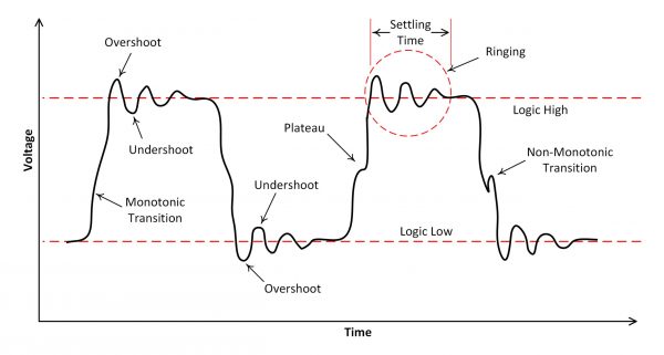
Design and optimization of PCB transmission lines are important tasks in the PCB design phase. These tasks must be incorporated into PCB layer stack design and demand interactions between PCB designer and PCB fabricator. Common PCB transmission line types for high-speed digital signals include:
- Microstrips (MS): PCB traces on top or bottom layer with an adjacent reference plane
- Striplines (SL): Inner layer PCB traces (on the same PCB stack layer) between two reference planes: one above and one below.
- Microstrips and striplines can be further divided into single-ended (SE) and differential MS / SL. Single-ended (SE) lines consist of a single trace. Differential lines consist of a pair of traces, and typically referred to as a differential pair (DP).
Designing the PCB Layer Stack for Transmission Lines
Multi-layer PCBs are typically selected for high-speed boards. Power and ground planes play a critical role in both signal integrity and power distribution network. These planes can be used as reference planes for the transmission lines.
For high-speed digital signals, the targeted transmission line characteristic impedances (Zo) are typically 50Ω (single-ended), 100Ω and 90Ω (differential). The achievable transmission line structures are determined by the PCB cross-sectional geometry, making layer stack-up design a complex process that must balance impedance control, routing density, and power delivery requirements.
Designing Transmission Lines for BGAs Under DFM Constraints
Ball Grid Array (BGA) packages are widely used for high-speed and high pin-count components such as processors, FPGAs, and switches. PCB designers must pay close attention to BGA breakout routing and multiple power supply rails during layer stack-up design.
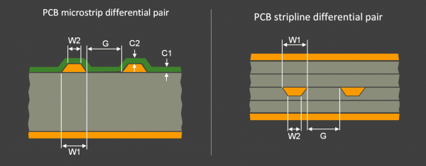
Designers often request that PCB fabricators provide a layer stack that includes every transmission line type on every signal layer (e.g. 50Ω single-ended, 100Ω and 90Ω differential pairs on every layer). However, this approach creates challenges for BGAs. On certain signal layers, achieving 50Ω single-ended widths may result in traces that are excessively wide, while achieving 100Ω differential pair widths may require traces that are too narrow. For example, on a PCB with a minimum 4mil/4mil trace/space, a 50Ω SE trace width may be set as 4mil, which means the corresponding 100Ω differential pair would need to be narrower than the 4mil on the same layer.
PCB designers should understand concept of minimal-routing-channel-width (MRCW) when designing stack-ups and transmission lines for BGAs. MRCW is defined by the space available between the BGA footprint pads on the external layer and by via-to-via spacing on internal layers.:
- MRCW for single trace: 1x trace-width + 2 x min. space, as a reference for SE.
- MRCW for a trace pair: 2 x trace-width + 3 x intra-pair space, as a reference for DP.
Instead of requesting both 50Ω SE and 100Ω DP differential pairs on every layer, designers can specify preferred combinations only on layers where they will be used.This approach gives the fabricator more flexibility in designing the stack-up so that transmission lines fit within the MRCW constraints.
Examples of Transmission Line and PCB Stack-Up Choices that Minimize BGS Impendence Mismatch
Start with 100Ω differential pair’s trace width and intra-pair space.
100Ω differential pair routing on one or more layers can fit into MRCW of BGA and follows the DFM guidelines for minimal trace width and conductor spacing as shown in Figure 1.
- The differential pairs are tightly coupled due to their small intra-pair spacing. The differential impedance remains consistent outside the BGA footprint. For a tightly coupled 100Ω differential pair, the impedance of each individual trace is higher than 50 Ω — typically up to around 60Ω.
- 50Ω single-ended trace routing, in this case, should fit into the MRCW with margin.
Figure 1: 100Ω differential pair routing can fit into MRCW of BGA.
100Ω differential pair routing, and a trace-pair with the minimal width and space cannot fit into MRCW of BGA on any layers as shown in Figure 2.
- Two 50Ω - 55Ω single-ended traces can be suggested for 100Ω differential pair in the layer stack-up. The 100Ω differential pairs will be loosely coupled with large intra-space.
- During BGA trace breakout, the two traces of a differential pair can be routed separately until they exit the BGA footprint, after which differential pair routing can begin. Within the BGA footprint, a differential impedance mismatch will occur
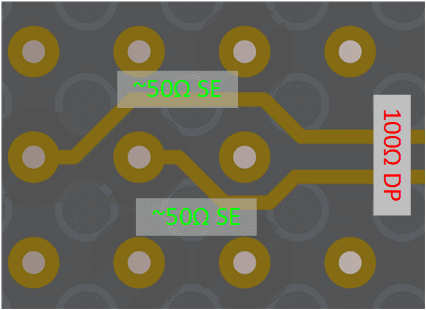
Figure 2: 100Ω differential pair routing, and a trace-pair with the minimal width and space cannot fit into MRCW of BGA. Single-ended traces are used for differential pairs within BGA footprint.
100Ω differential pair routing cannot fit into MRCW of BGA on any layers but routing for two a trace-pair (Zdiff ≠ 100Ω) can fit into the MRCW under the DFM guidelines for minimal trace width and conductor space as shown in Figure 3.
- During BGA trace breakout, the “differential pairs” with different impedance from 100Ω can be routed until they exit the BGA footprint, after which standard 100Ω differential pair routing can begin. Within the BGA footprint, a differential impedance mismatch will occur.
- 50Ω single-ended trace routing, in this case, should fit into the MRCW with margin.
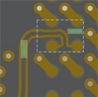
Figure 3: 100Ω differential pair routing cannot fit into MRCW of BGA. But a trace-pair with minimal width and space can fit into the MRCW.
Managing Crosstalk Between Adjacent Signal Layers
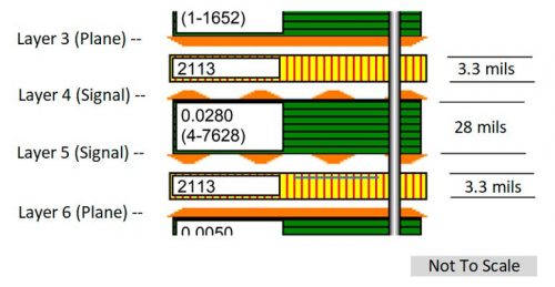
Two adjacent internal signal layers are often used in cost-effective, multilayer high-speed PCBs. The following are design and layout practices are recommended to minimize crosstalk between these layers.
- Keep the distance between the adjacent signal layers as large as possible in the layer stack-up.
- Keep the signal layers close to their reference planes when possible in the layer stack-up.
- Include a PCB layout note for trace routing (e.g. “Traces on Layers 4 and 5 should be run perpendicularly”).
Understanding High-Speed Signal Loss in PCBs
It is important to understand the different sources of loss in PCB transmission lines when selecting materials for high-speed signals:
- Conductor loss, DC and AC: associated with conductor cross-section and length, and skin effect for the high frequency components.
- Dielectric loss and Df: selecting the material with the lower Df (dissipation factor) to reduce signal attenuation from dielectric losses.
How PCB Layer Stack-Up Impacts EMC Performance
One effective technique for suppressing EMI on high-speed PCBs is to reduce the current loop area. For most digital signals, the loop follows this path: Driver → PCB trace → Receiver → PCB Current Return Path → Driver. For PCB transmission lines, the reference planes serve as the current return path.
When designing the PCB layer stack for EMC, the following considerations should be taken into account:
- The reference plane should be as close as possible (using a thin dielectric) to signal layers to minimize the loop area.
- When possible, use power and ground plane-pairs in a PCB layer stack (for example, +3.3V and GND). These plane pairs should be placed closed together to minimize the plane inductance and increase plane coupling capacitance.
- Position reference planes next to top and bottom layers and assign them as ground planes whenever feasible
Pre-Layout SI Simulation and Its Role in High-Speed Design
Pre-layout SI simulation tools working with PCB layer stack-up are recommended. The PCB design team should provide the tools with as much information as possible about the transmission lines, including the stack-up, placements of the drivers and receivers, component packages, and any additional details needed to ensure simulation accuracy relative to the final PCB layout.
Pre-layout SI simulation can help PCB design team with:
- Reviewing interconnect design margins for worst-case conditions.
- Reviewing distance between drivers and receivers based on eye diagrams (eye height).
- Setting timing margins for PCB trace length matching based on eye diagram (eye width).
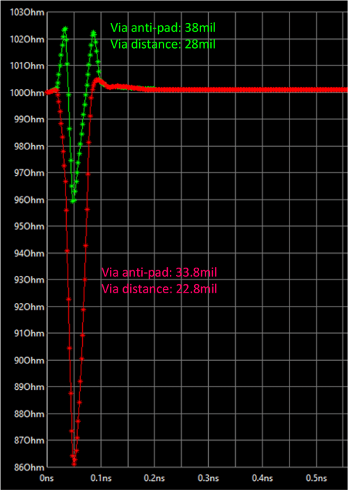
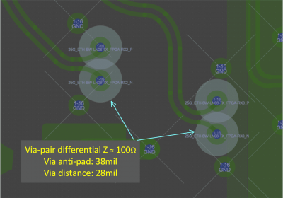
- Optimizing single via and via-pair impedances by adjusting via hole size, pad geometry, anti-pad shape, and via placement patterns.
- Establishing trace routing guidelines to minimize crosstalk and impedance-mismatch.
- Optimize transmission line terminations.
An example of via-pair impedance optimization: The green plot has much less impedance mismatch to 100Ω.
Pre-layout (schematic) simulation, in fact, can be extended into the PCB layout phase. By incorporating component placementand trace-breakout schemes, pre-layout simulation produces results that more closely reflect the actual PCB layout.
Once pre-layout considerations are addressed, the focus shifts to layout execution.
PCB Layout Practices for Signal Integrity
In PCB design, whether a digital signal is classified as high-speed depends on the signal’s rise time or fall time (tr) and the propagation delay along its interconnect (tpcb), which is primarily determined by PCB trace length between the driver and the receiver. When ratio tpcb / tr > 1/5 (or 0.2), the signal should be categorized as high-speed.
For a signal with tr = 2ns, the following examples illustrate this:
- tpcb = 600ps: This corresponds to approximately a 4 inches long PCB trace on outer layer (Td = 150ps/in). Since tpcb / tr = 0.3 > 0.2, the signal should treated as high-speed.
- tpcb = 150ps: This corresponds to apprixmately a 1 inch long PCB trace on outer layer. Since then tpcb / tr = 0.075 < 0.2, the signal can be treated as low-speed.
For the signals connected to the large packages, such as 25mm x 25mm BGAs, with rise times of hundreds of picoseconds, they should always be treated as high-speed because the propogration delay includes both the PCB trace and the package itself.
During layout placement, PCB designers should review digital signals that do not include termination. If drivers and receivers without terminations cannot be placed close together, then transmission line design and termination may become necessary.
Transmission line termination involves matching impedance at both ends of the transmission line. Terminated transmission lines have the lowest RF energy emission and are beneficial to PCB layout EMC. In point-to-point topologies, a driver is located at one end and a receiver at the other. In multiple-drop topologies, drivers and receivers may be placed anywhere along the transmission line.
On-die termination (ODT) for drivers and receivers is recommended over discrete termination on the PCB. If discrete termination is used, it should be placed and connected appropriately.
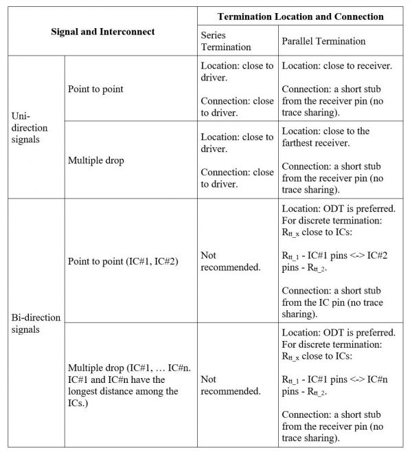
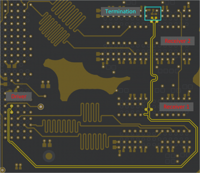
An example of termination for a differential clock: single driver with two receivers.
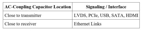
Placement Guidelines for AC-Coupling Capacitors
AC-coupling capacitors are required for certain high-speed differential signaling interfaces. Placement recommendations are typically provided in the corresponding interface specifications, and PCB designers should follow the guidelines from IC manufacturers.
The table below summarizes general placement guidelines for AC-coupling capacitors.
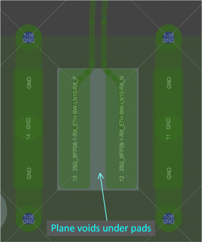
Footprint pads and vias introduce impedance discontinuities in the signal path. PCB designers can apply specific layout techniques to compensate the mismatches and minimize discontinuities.
Adding a plane void placed under a footprint pad (i.e. on the adjacent plane layer) reduces capacitance between the pad and the plane. This compensation technique applies to pads in the footprints of SM IC packages, SM connectors, AC-coupling capacitors, and similar components.
Example for component footprint pads:

Example for connector pads:
SI simulation tool is needed to provide impedance compensation guidelines on PCB single vias and via-pair. PCB designers should understand that via impendence is influenced not only by the hole size, pad size, and via spacing, but also by the via stub length, anti-pad, and overall PCB layer stack-up.
PCB Layout for Timing Margins and Delay Matching
Propagation delay (time delay) in PCB transmission lines is approximately 150ps/in for microstrips and180ps/in for striplines. For a 6 inch long transmission line, the time delay in the PCB trace is approximately 0.9ns for microstrips and 1.1ns for striplines. Differences in trace lengths cause differences in time delay that affect:
- Time margins for synchronous bus
- Differential signal timing skew and mode conversion
PCB trace time delay tuning tools can often incorporate IC package time delays. The firmware or FPGA teams should be consulted before including package time delay in the PCB tuning because development and debug tools may already account for these delays during timing verification.
Time delay matching (also known as trace length matching or tuning) should be implemented during PCB layout in order for the PCB time delay to not negatively impact overall digital system timing margins and budgets. Time delay in PCB interconnects can include traces, pads, vias and delays within IC packages.
One effective approach is to match trace delays across all signal paths (if package time delay can be ignored). After the tuning, all the PCB time delays become the same and time delay differences are near zero. This allows the PCB time delay differences to be excluded from the system timing budget unless specific PCB time-delay elements are required.
PCB Layout Practices for EMC Performance
PCB layer stack-up, component grouping and placement, and the PCB layout – especially, for the external signals and connectors – are key areas for EMC layout review. Grounding methods for external connectors, wire cables, and enclosure are a part of system-level design and play an important role in EMC performance. The chosen grounding method, or combination of methods, should be clearly defined in design documentation.
- Place the drivers / receivers for external signals close to the connectors.
- Consider placing cutouts in the PCB power planes within the areas at the external connectors. It helps in reducing plane-to-plane or/and plane-to-signal coupling to the external signals.
- Strategically plan the locations of the low-speed and high-speed signals entering and their ground connections to the areas for the external signals and connectors.
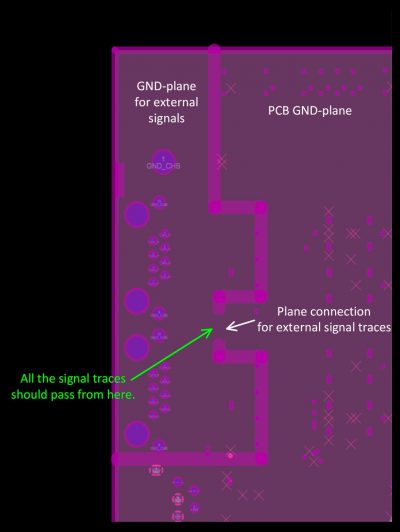
- For the external connectors, as needed, employ long plane slots to break the solid plane and create the designated connection between “external-signal ground plane” and the PCB ground plane as illustrated below. The external signals should enter the connectors at the plane connection.
Additional EMC Layout Considerations
Component Placement
- Group the high-speed circuits as blocks.
- Place the high-speed blocks away from connectors.
- Place clocking circuits (blocks) away from connectors.
- Place ESD, EMI-suppression components close to connector pins.
- Place de-coupling capacitors close to the power pins.
PCB Layout
- Keep the adjacent reference plane(s) for the high-speed traces (transmission lines) as solid planes when possible (i.e. avoid segmented planes).
- Avoid routing signals across slots (gaps) in the reference planes, as well as the voids caused by anti-pad to vias, through-holes.
- Use striplines (internal layers) for high-speed signals and clocks when possible.
- Avoid routing high-speed traces near PCB edges.
- Place ground polygons on the top and bottom layers. Place ground vias along PCB edges to connect the top and bottom polygons, as well as the internal ground planes.
Conclusion
During the pre-layout design phase for the high-speed PCBs, transmission line design becomes challenging when combined with the need to minimize impedance mismatch while meeting DFM constraints. This combination has become one of the critical aspects of PCB layer stack-up design for the high-speed boards. It is also recommended that PCB layout guidelines for crosstalk, impedance compensation, and time delay tolerances be established before PCB trace routing begins. These guidelines can come from experienced PCB design engineers or be derived from SI simulation tools based on the recommended PCB layer stack-up.
In the PCB layout phase, two key SI layout tasks are particularly important: implementing impedance compensation for footprint pads and vias, and tuning trace routing to match time delays. In some cases, the time delay in the driver and receiver packages must also be included in the overall timing analysis.
EMC design is closely tied to signal integrity. Most SI design practices naturally improve EMC performance. Inadequate SI design not only compromises signal quality, it often results in poor EMC performance. Component placement for EMC design is primarily focussed on minimizing coupling between high-speed circuits and external interconnects. EMC-focused layout should aim to minimize current loop areas for the high-speed signals, including both signal traces and their return paths.
Navigating SI and EMC challenges in high-speed PCB design requires deep technical expertise and careful planning. At Nuvation Engineering, our team combines simulation-driven design with proven layout practices to help clients avoid costly performance issues and ensure compliance. If you’re developing a high-speed system, now is the time to engage with a team that understands how to design for performance and compliance from the ground up
Key Takeaways
- SI and EMC issues often appear late in the design cycle, but are best addressed early.
- Simulation and PCB design expertise are essential for achieving reliable performance in high-speed PCBs.
- The pre-layout design phrase is critical for developing cost-effective high-speed PCBs with reliable SI and EMC performance.
- Nuvation’s design practices help avoid costly delays and compliance risks.