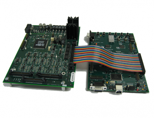
Designing high-speed, high-density digital, analog, and RF PCBs for diverse applications.
Schematic Capture
From concept to production, we create precise schematics that drive reliable electronic hardware development.
First-Time-Right PCBs
Delivering successful first-build PCB designs with high signal accuracy and layout precision.
Software & FPGA Design
Creating embedded software and FPGA solutions alongside hardware development efforts.
Advanced PCB Analysis
Providing peer reviews, signal integrity modeling, and PDN analysis upon client request.
Manufacturing Readiness
Ensuring a smooth transition from prototyping to volume production and certification.
Our Experience
PCB Design Expertise
High-speed, multi-layer digital PCB designs (SMT, SMT/TH and HDI), e.g. Fibre channel FC8, FDR InfiniBand, PCIe 4.0, HDMI 2.0, SATA 2.0, XAUI, USB3.2, Thunderbolt, DisplayPort, MIPI CSI-2, 25GbE, DDR4
High-speed SerDes circuits up to 25GHz (single lane)
High-speed MIPI CSI-2 circuits for multiple cameras / images
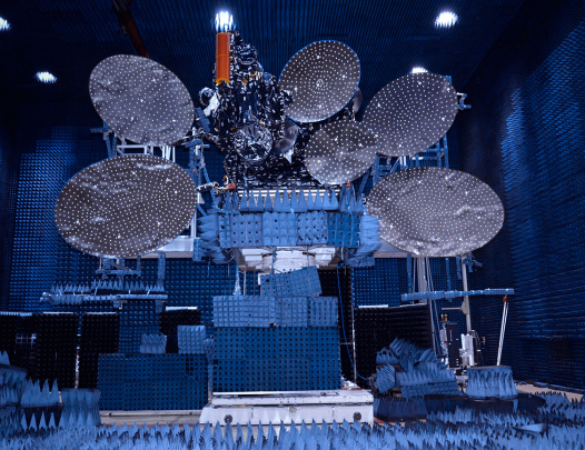
Radio frequency (RF) PCB designs
High-speed data bus memories, e.g. DDR2/3/4/5/6, QSPI, NOR/NAND Flash, SRAM, proprietary buses
High-speed optical signal circuits, e.g. ROSA, TOSA and SFP28 (25Gbps)
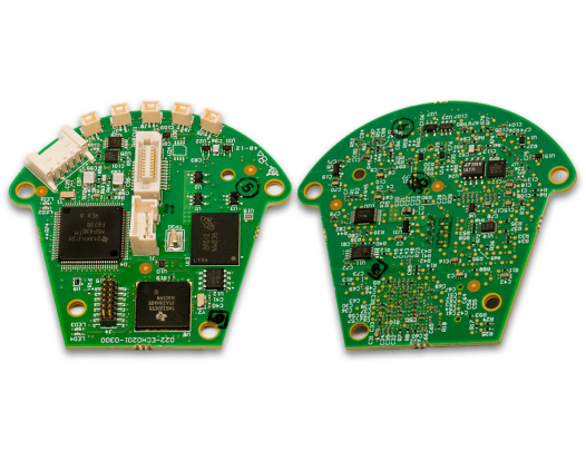
High-density and high pin-count designs in advanced PCB technology, e.g. microvias, via-in-pad, ultra-fine pitch BGAs, ‘first-time-right’ and DFM methodologies
Any-layer HDI PCB for boards with ultra-fine and high pin-count packages
Low-level analog PCB designs
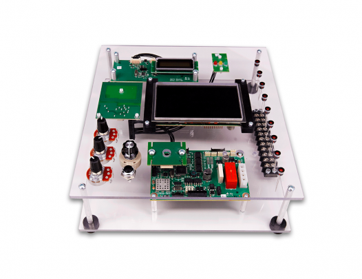
Test fixture PCBs
Rigid-flex PCB
Memory interfaces, e.g. DDR2, DDR3, DDR4
Mixed-signal boards requiring noise / power isolation
PCB Signal and Power Integrity: pre- and post-layout analysis and verification
Impedance-controlled, transducer-interfacing, and sensitive signal designs